Since a few years, it is possible to isolate sheets with thickness of an atom and width of dozens of micrometers. It is possible to proceed with metallic, insulating, or semi-conductors materials and to assemble them in various heterostructures. The new 2D transitions metal dichalcogenide (TMDs) as MoS2 represents ideal material for multiple purposes. It is promising for electronic transistor and fundamentals phenomena such as superconductivity or valleytronic. It is a rich platform for optoelectronic; excitonic effects have high binding energy, strain engineering can induce a high tunability of the band gap itself and these materials are also interesting for the study of electron-holes liquid phase at room temperature. Moreover, these materials transit between different crystalline phase (2H-1T) making this material interesting for memristive devices and energy storage.
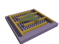
Our activities focus on the design, the fabrication and the electronic properties of novel hybrid heterostructures based on two-dimensional materials (graphene, and transition metal dichalcogenides), in view of the realization of a new generation of nanoelectronic devices. We study the electronic level alignment between the top and bottom layers of various interfaces. The theoretical background of this study relies on the careful consideration of the van der Waals interaction that is at the origin of the stacking between the different layers. We also study a new sample type with large suspended monolayer MoS2 with electrical contacts. This type of hybrid structure of opto-electro-mechanic (NOEMS) couples at the same time the nanomechanics with interesting properties of the large 2D materials.