![]()
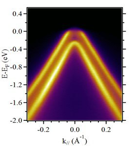
Figure: Above; ARPES measurements of a epitaxial bilayer graphene. Below a diode made with a junction between a Monolayer Mos2 flake and a graphene layer
The C2N is a Paris Saclay-CNRS research organization hosting groups in the fields of material science, mesoscopic physics, microfluidics, optics and photonics and has its own nano-fabrication facility, located in more than 3000 m² of (class 1000/100) clean rooms. The group Mat2D at C2N is expert in the growth of carbon structures and of transition metal dichalcogenides. This group also has a recognized expertize in surface techniques like Angular resolved Photo Emission Spectroscopy (ARPES), Low-energy electron microscopy (LEEM) and STM/STS, and in technological processing of samples (clean room facility). Experiments using the above-mentioned techniques will be performed at C2N and synchrotron Soleil.
