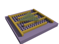
Our research focuses on the controlled growth and fundamental properties of two-dimensional (2D) materials and their heterostructures. We develop complementary approaches based on chemical vapor deposition (CVD) and molecular beam epitaxy (MBE) to achieve high crystalline quality, precise thickness control, and engineered interfaces. CVD enables the scalable synthesis of large-area monolayers and alloys of transition metal dichalcogenides (TMDs), while MBE provides unparalleled control over layer-by-layer growth, stacking sequence, and interface sharpness. These techniques allow us to access metastable phases, tailor polymorphism, and fabricate quasi-van der Waals heterostructures with reduced interlayer coupling or, conversely, enhanced hybridization.
A central aspect of our work is the investigation and engineering of the electronic band structure in 2D systems. Using a combination of advanced spectroscopies and device-based approaches, we probe band dispersion, band alignment, and many-body effects in semiconducting and metallic TMDs and their alloys. Particular attention is given to the evolution from monolayer to bulk, the role of symmetry and stacking (e.g., 2H vs 3R phases), and the emergence of interfacial states in heterostructures. By controlling composition, thickness, and environment, we tune band gaps, spin–orbit coupling, and valley-dependent properties. Confinement effects—whether arising from reduced dimensionality, quantum wells, or nanoscale patterning—are exploited to access new electronic and optical regimes, including enhanced excitonic effects and modified carrier dynamics.
Beyond static properties, we explore the coupling between mechanical deformation and electronic structure in the emerging field of straintronics. Strain provides a powerful and reversible knob to modulate band structure, induce pseudo-magnetic fields, and control carrier localization at the nanoscale. We also investigate thermal transport in suspended and supported 2D systems, where reduced dimensionality, strong anharmonicity, and interface effects lead to unconventional heat conduction. Understanding and controlling heat flow is essential for both fundamental insights and the development of efficient nanoelectronic and optoelectronic devices.